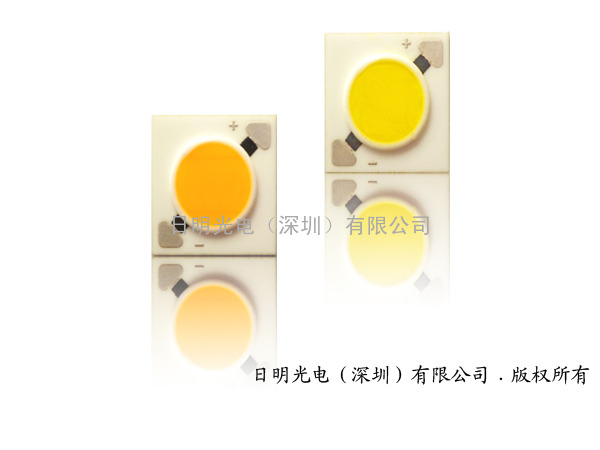
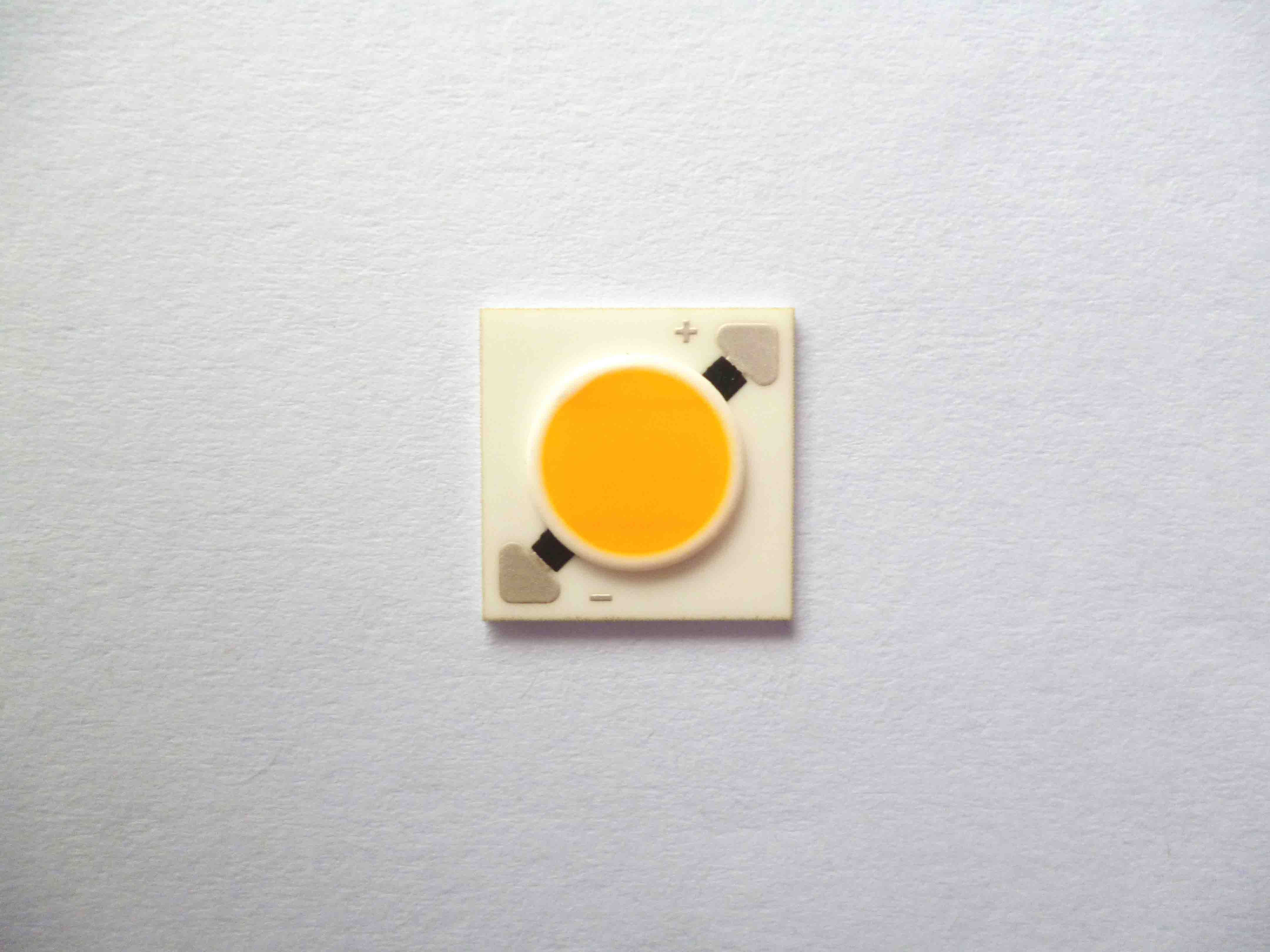
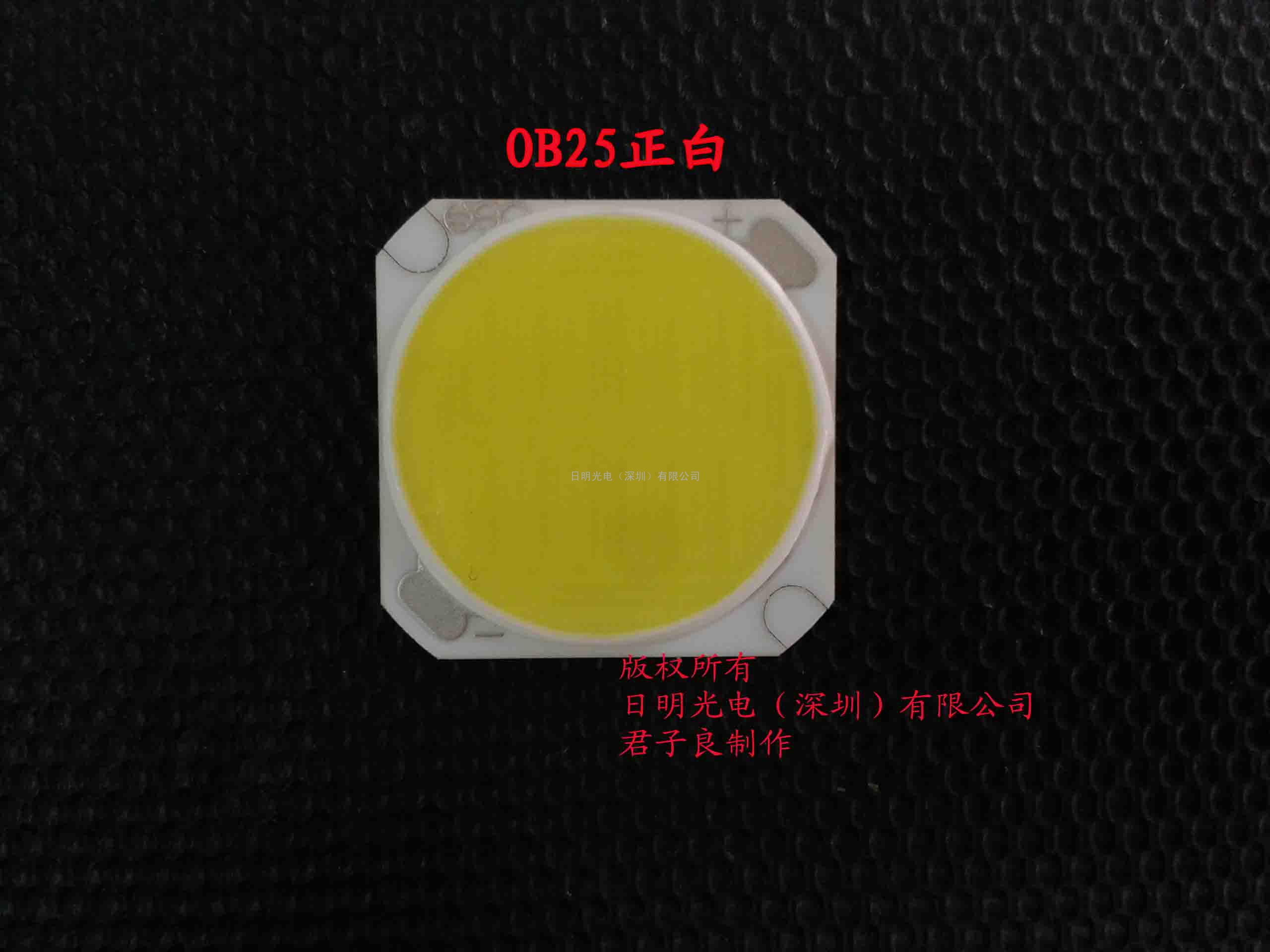
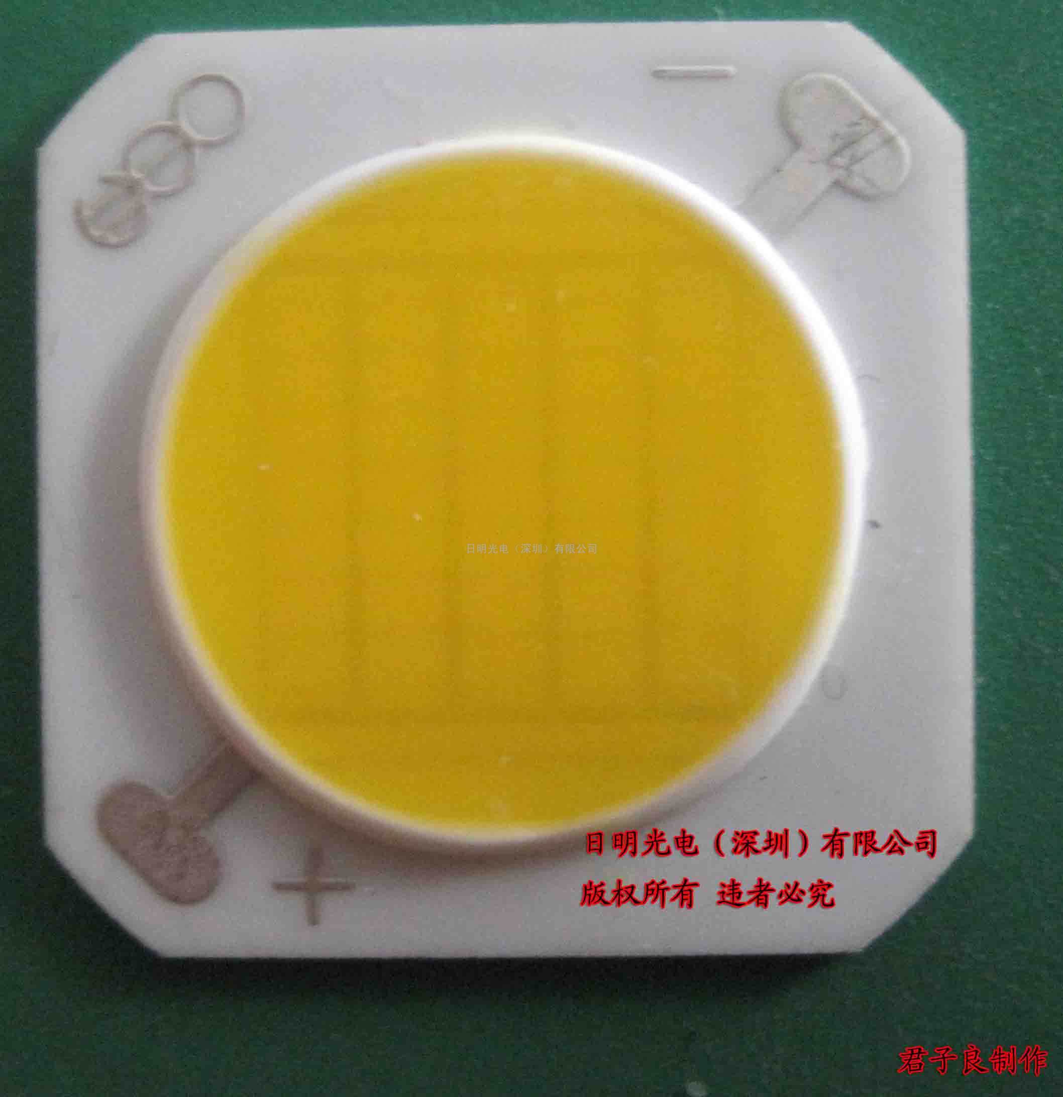
With this technology, the LED chips are in the form of a semiconductor chip (die) size between 100~200 micron. The individual chips are placed on the ceramic substrate PCB and using the Wire Bonding method, connected to the contact surface of the ceramic substrate PCB. Gold wires in the micrometer range are used for contacting the semiconductor chip and the substrate. The COB technology allows for virtually limitless *** of scope for the PCBs and thus serves as the basis for totally unique LED soluti***. Furthermore Lumiere is using ceramic as substrate of which will improve the internal quantum efficiency and increase heat dissipation. The careful design of the ceramic PCB and selection of quality dies in c***equences minimize electrical losses and light extraction on the dies and improve the LED efficiency.
1.高热导陶瓷基板,芯片所产生的热量可迅速通过陶瓷基板向外传导
2.高显色指数,高发光效率发光均匀,
3.光线柔和,无眩光,无光斑高可靠性,额定工作电流下,5000小时衰减低于3%
4..发光均匀,光线柔和,无眩光,无光斑 5..组装方便,可自由搭配和组合,无需PCB板,直接接触散热片。

