


Key Features
*VDD = 1.8 +/- 0.1V
*VDDQ = 1.8 +/- 0.1V
*All inputs and outputs are compatible with SSTL_18 interface
*8 banks
*Fully differential clock inputs (CK, /CK) operation
*Double data rate interface
*Source synchronous-data transaction aligned to bidirectional data strobe (DQS, DQS)
*Differential Data Strobe (DQS, DQS)
edges when read (edged DQ)
*Data outputs on DQS, DQS
*Data inputs on DQS centers when write(centered DQ)
transition with CK transition
*On chip DLL align DQ, DQS and DQS
*DM mask write data-in at the both rising and falling edges of the data strobe
*All addresses and control inputs except data, data strobes and data masks latched on the rising
edges of the clock
*Programmable CAS latency 3,4, 5, 6 and 7 supported
*Programmable additive latency 0, 1, 2, 3, 4 and 5 supported
*Programmable burst length 4/8 with both nibble sequential and interle***e mode
*Internal eight bank operati*** with single pulsed RAS
*Auto refresh and self refresh supported
*tRAS lockout supported
*8K refresh cycles /64ms
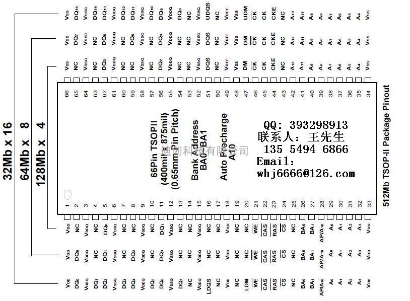
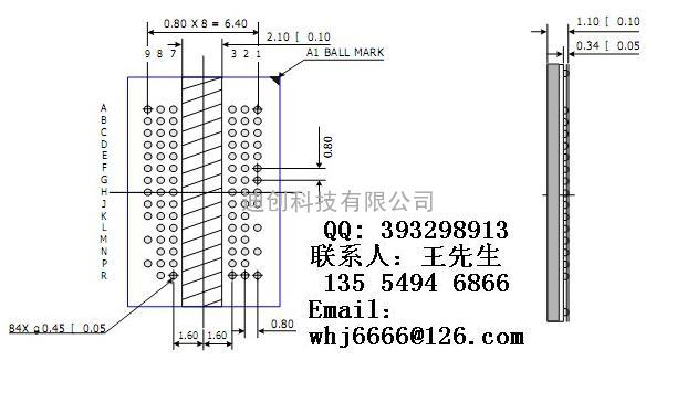
*JEDEC standard 84ball FBGA(x16)
*Full strength driver option controlled by EMR
*On Die Termination supported
*Off Chip Driver Impedance Adjustment supported
*Read Data Strobe supported (x8 only)
*Self-Refresh High Temperature Entry
****erage Refresh Period 7.8us at lower than Tcase 85C, 3.9us at 85C<Tcase<95C
若贵司有产品上的疑问或详细规格上的需求,希望能与我们联络。以上的资讯,提供给您,也欢迎转寄贵司相关人员作为参考。敬祝贵公司业务宏图大展,谢谢。
迪创科技有限公司 DigiTron Technology Limited
地址:香港荃灣青山道264-298***南豐中心1522室
联系人: 王先生 手机:联系人:135 5494 6866
电话:0755-22900421 传真:0755-22900423
Email:whj6666@
***: 393298913
MSN: t-con2010@
深圳***:深圳市罗湖区笋岗东路2121号808